
A new manufacturing technology developed by Demcon Photonics is set to enable the scaling up of photonics to large-scale industrial production. The method offers an alternative to the existing method for actively aligning optical fibres with photonic chips. The new approach utilises direct laser writing, which allows optical connections to be precisely etched into glass. According to Demcon, this results in a faster, more reliable and more scalable production process.
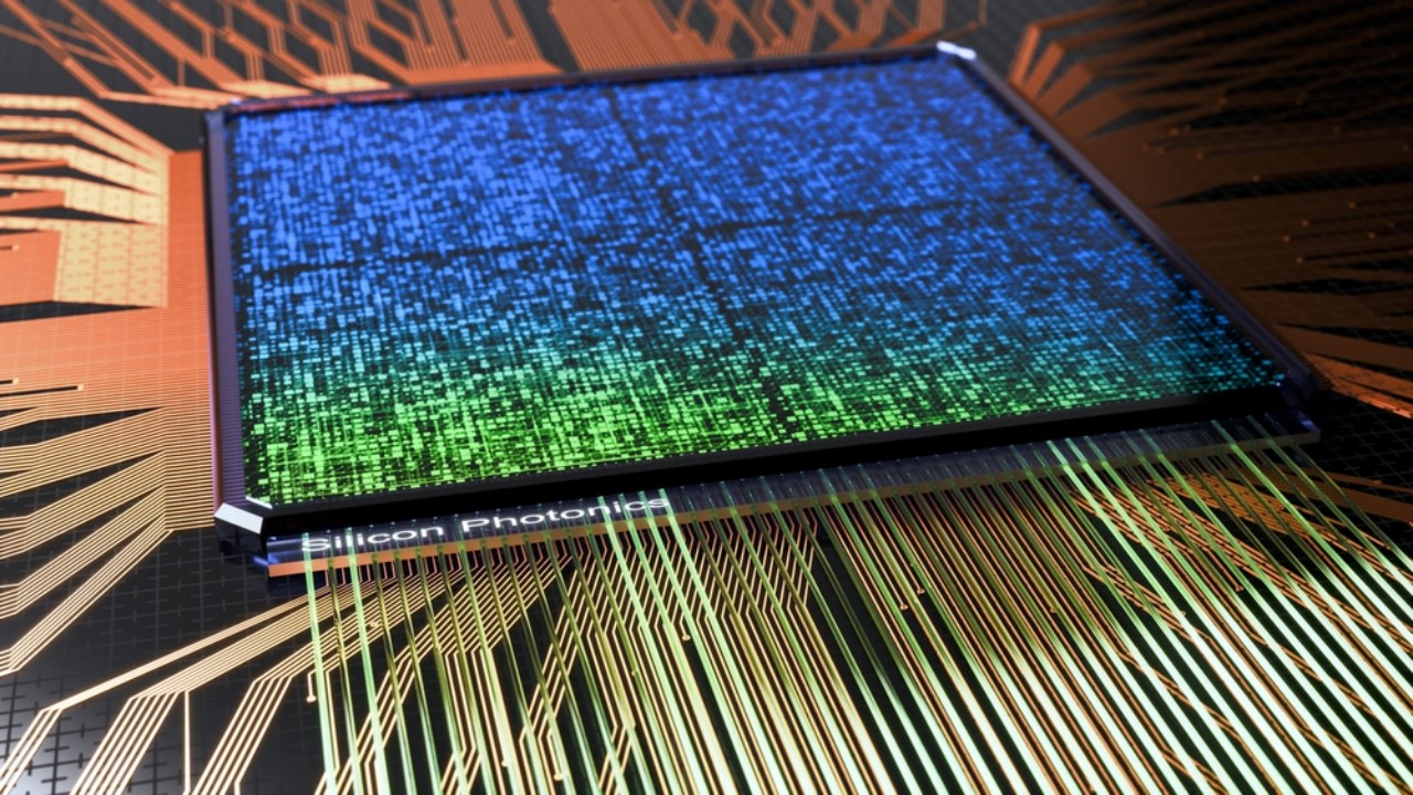
Photonics is a technology that uses light to transmit, process or detect information. Whereas electronics rely on electrical signals and electrons, photonics utilises particles of light: photons. Photonic integrated circuits (PICs) represent a major development in the field of photonics. These chips combine various optical functions on a single chip, similar to the integration of various electronic components on a microchip. Photonics offers possibilities for, amongst other things, high-speed data transmission, energy-efficient data communication, advanced sensors and medical applications. The technology is playing an increasingly important role in fields such as data centres, telecommunications and high-performance computing.
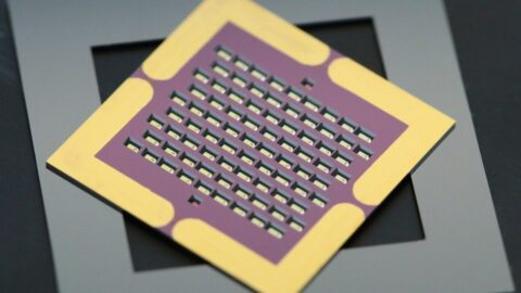
Scaling up photonic production requires the precise alignment of optical fibre arrays with photonic integrated circuits. In the existing method, fibres are actively aligned relative to the chip. However, this process is relatively time-consuming and limits the scalability of the production process. Distortions can also occur in both the optical fibre arrays and the photonic chips, which can affect the reliability of the alignment process. The latter is particularly relevant when only a limited number of fibres are used to determine the alignment of an entire array.
Direct laser writing as an alternative
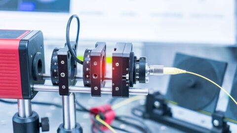
Demcon Photonics is investigating the use of direct laser writing as an alternative to active fibre alignment. With this technique, optical waveguides are written directly into glass using ultrashort laser pulses from femtosecond lasers. These waveguides form the connections between the optical fibres and the photonic chip.
To determine the positions of the connections accurately, the individual fibres and the interfaces of the photonic chip are first measured using computer vision. Based on this measurement data, the laser can create the optical connections at the correct locations. This results in a method in which the coupling between optical fibres and chips is less dependent on conventional active alignment.
Direct laser writing is, incidentally, not a new technology. The method has long been in use in fields such as microfluidics, glass processing and surface treatment. Demcon Photonics aims to further develop the technique and adapt it for the production of photonic components. Its objective is to achieve a fast and reproducible process with minimal optical coupling loss, suitable for larger production volumes.
The Dutch photonics industry is developing rapidly
In recent years, the Dutch photonics industry has taken concrete steps to scale up the production of photonic chips. In addition to investments in the ecosystem, new research facilities and industrial pilot production lines are being developed. A key initiative is PIXEurope, a European programme for the development of production facilities for integrated photonics. As part of this initiative, work is underway in Eindhoven on an industrial pilot production line for photonic chips based on indium phosphide (InP). Production is being scaled up to 6-inch wafers. TNO, Eindhoven University of Technology, the University of Twente and the Photonic Integration Technology Centre (PITC), amongst others, are involved in the project. The facility is intended to accelerate the transition from research to industrial production and is due to be operational by 2027. Approximately 153 million euros is being invested in the Eindhoven production line.
The national PhotonDelta programme is also actively supporting the development of the photonics sector. The focus here is on expanding the Dutch ecosystem for integrated photonics. In December 2025, for example, eighteen research projects were selected for funding by the Netherlands Organisation for Scientific Research (NWO) and PhotonDelta. In total, over 16 million euros is available for research into, amongst other things, photonic materials, components and systems.
In addition, TNO and ASML entered into a partnership in June 2026 to further develop and test lithography, process control and measurement technology at a new pilot facility in Eindhoven. The aim is to accelerate the industrialisation of photonic chips.
Demonstration model planned for 2027
Demcon Photonics is currently working on prototypes of the new production method. The company aims to present a demonstration model to potential collaboration partners in early 2027. Among other things, this model is intended to demonstrate the applicability of direct laser writing for the optical interconnection of fibre-optic arrays and photonic chips.